
Electron microprobe edit
An electron microprobe (EMP) was invented in 1951 by Raymond Castaing (1921-1998) in France as a nondestructive method for chemical analysis of surfaces of solid samples. A focused electron beam is applied to excite characteristic X-rays revealing the identity and approximate concentrations of chemical elements present in the sample. The resolution, limited by the spreading of the electron beam, is ~1μm and all elements heavier than boron (Z=5) can be detected to a level as low as 100 ppm.
History edit
The history of the electron microprobe goes as far back in the history as to the discovery of characteristic X-rays (Charles Glover Barkla and Charles A. Sadler, 1909), the invention of the crystal diffraction spectrometer (Bragg and Bragg, 1913) and the construction of the first electron microscope (Ernst Ruska and Max Knoll, 1931).[1], [2], [3]
Development of the electron microprobe was preceded by that of the closely related analytical technique of X-ray fluorescence spectrometry (XRF). This technique was first proposed by Georg von Hevesy in 1923 and applied by other workers in the following few years.
In 1944, MIT built an electron microprobe, combining an electron microscope and an energy-loss spectrometer. Electron energy-loss spectrometry is very good for light element analysis and they obtained spectra of C-Kα, N-Kα and O-Kα radiation. In 1947, Hiller patented the idea of using an electron beam to produce analytical X-rays, but never constructed a working model. His design proposed using Bragg diffraction from a flat crystal to select specific X-ray wavelengths and a photographic plate as a detector.
In 1948-1950, Raymond Castaing, a graduate student supervised by Professor André Guinier at the University of Paris, France, built the first electron “microsonde électronique” (electron microprobe) at the University of Paris. This microprobe produced an electron beam diameter of 1-3 μm with a beam current of ~10 nanoamperes (nA) and used a Geiger counter to detect the X-rays produced from the sample. However, the Geiger counter could not distinguish X-rays produced from specific elements and in 1950, Castaing added a quartz crystal between the sample and the detector to permit wavelength discrimination. He also added an optical microscope to view the point of beam impact. The resulting microprobe was described in Castaing's 1951 Ph.D. thesis, in which he laid the foundations of the theory and application of quantitative analysis by electron microprobe, establishing the theoretical framework for the matrix corrections of absorption and fluorescence effects (“ZAF”). An independent development of an electron microscope was carried out in the former USSR by Borovskii (1953).
Cameca Company in France produced the first instrument “MS85”, in 1958. Soon, it was followed by other companies, such as, AEI Ltd in the UK (Page and Openshaw, 1960) and ARL Inc. in the USA (O’Brien, 1963). Based on the works by Cosslett and Duncumb (1956) and Duncumb and Melford (1960), the Cambridge Instrument Company developed the “Microscan”, an instrument that produced visual element distribution images in a TV-like mode. JEOL company in Japan came to the market with a scanning electron microscope. Other significant modifications and improvements included the development of the solid-state lithium-drifted silicon, Si(Li), detector (1968), the energy dispersive (ED) analysis (Tenny, 1968) and the development of synthetic multilayered diffracting materials for the detection of light elements. Cameca and JEOL are now the only ones on the market.
How it works edit
Components edit
The basic components of an electron microprobe are: electron gun, two or more sets of lenses, sample holder and an X-ray analyzer, which can be either an energy-dispersive spectrometer or wavelength-dispersive spectrometer (EDS and WDS, respectively). The electron gun contains a tungsten filament, which is heated to ~2700 K and held at a negative potential, typically 10-30 kV. The electrons accelerate through a small aperture in an earthed anode plate. Keeping the chamber under high vacuum (10-4 Torr or better) prevents from the oxidation of the tungsten filament, breakdown of the accelerated voltage, and scattering of the electrons within the beam. The electron beam is then focused through the magnetic lenses and demagnified by the electron lenses (more sets of lenses are used for high resolution scanning images). The current of the electron beam can be mostly affected by the optical lenses; the closer the lenses are to the specimen the analytical quality increases but imagining capability decreases. As the electron beam hits the specimen X-rays are generated in the sample. The wavelength (recorded in WDS) or photon energy (recorded in EDS) is characteristic of each chemical element, while the intensities in the X-ray spectrum are used for quantitative analysis by reference to standards.
-
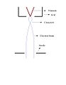
 Schematic diagram of an electron microprobe.

A conventional triode gun contains a hairpin shaped tungsten wire filament, which constitutes the cathode and it is at a high negative potential relative to earth. Other primary components of a gun are a grid (“wehnelt”) kept at a negative potential of a few hundred volts relative to the cathode and lastly an earthed anode plate containing a small aperture of few millimeters in diameter; Fig. 2. The tungsten filament possesses the advantages of having a fairly low work function (4.5 eV) and a high melting point (3643 K). Thus it can be comfortably heated to 2700 K and emit electrons thermionically. An alternative to tungsten filament is lanthanum hexaboride (LaB6). This material has an even lower work function (2.2 eV) thus allowing for a higher current density at a lower temperature than the tungsten filament. LaB6 also offers more than 10-fold increase in brightness, a highly desired effect in scanning electron microscopy, where the visual quality comes before the analytical aspects. On the negative side, lanthanum hexaboride increases in reactivity at elevated temperatures.
-
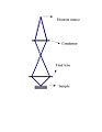
 The path of the electron beam in a gun.

As the pathway of the electron beam in a gun indicates, a lens is required to demagnify the crossovered electron beam. The first lens is called the “condenser” and the last lens is referred to as the “final” lens. Optical systems may contain an additional condenser lens to improve the scanning quality. The focus of the scanned image depends on the final lens, while the size of the image of the source formed on the surface of the sample is directed by the condenser lens; Fig. 3. Two types of lenses can be used: magnetic and electron lenses. The magnetic ones are preferred due to lower aberrations. They are composed of copper coils covered with an iron layer.
-
 Two-lens demagnifying optical system.

Wavelength-dispersive analysis (WDA) edit
X-rays edit
As the specimen is bombarded by the electrons, X-rays are produced and the X-ray spectrum is recorded. The incident electrons collide with the electrons in atoms that cross their path (the specimen) and consequently decelerate, thus producing a continuum radiation spectrum. Out of all the collisions, some electrons will collide with electrons in the inner orbital of an atom, ejecting the inner electron and creating a vacancy. Other electrons from outer orbitals will then fall into the vacancy, emitting energy corresponding to the difference in the electron energy levels. Such radiation is called “the characteristic radiation” and it will show as a sharp peak in the X-ray spectrum. These lines are labeled with capital letters K, L, M..., Greek letters α, β, γ... and subscripts 1, 2..., representing each specific electron transition within atoms; example: Kα1 is a transition from L3 to K level. Elements can be identified based on these characteristic radiation lines. The wavelength of an ejected electron can be determined from the Bragg’s law,

where λ is the wavelength, n is the order of reflection, d is the spacing between the atomic planes and θ is the angle of incidence. Since the bombardment of the specimen produces a continuum X-ray spectrum, a filter also called a monochromator is required to select only the characteristic radiation of a specific wavelength. For that purpose, a crystal of known diffraction parameters with diffracting planes parallel to the surface is mounted between the sample and the detector. From the Bragg’s law it implies that at a given angle θ only one wavelength can satisfy the law. Crystal is then rotated to obtain multiple values of wavelength (the range of wavelength is limited by the nature of a specific crystal in use). From there comes the name wavelength-dispersive analysis. In order to obtain a wide range of wavelengths a series of spectrometers with different crystal parameters are used. The main advantage of WDA over EDA is the analytical sensitivity of very long wavelength (low energy) spectra; the EDA in this region fades within the background signals. It provides crucial improvements in detection of ultra light elements (down to boron).


Crystals edit
Different crystals are being used to satisfy the analytical needs. The important factor of the crystals is the so called “integrated reflectivity” (Ri), which is defined as the area of the curve of reflectivity against the angle θ. The reflectivity of perfect crystals typically ranges between 10-4-10-5 rad. Some real crystals have higher reflectivity than a perfect crystal. This is explained by the slight imperfections in the internal orientation of subunits of the crystal domain, thus increasing the range of wavelengths that would satisfy the Bragg equation. Other means of increasing the reflectivity is to abrade the surface of a crystal or to use a doubly curved crystal. Some natural crystals that were used include rocksalt, mica, calcite and quartz. Later, synthetic alternatives were well adapted, by combining the best physical properties (curvature; thickness; response to vacuum, temperature and moisture, etc.). Lithium fluoride, LiF, is used as the standard crystal for short wavelengths (less than 3 Å), pentaerythritol (PET) is common with medium wavelengths and acid phthalates for long wavelengths. These crystals cover the range of approx. 1-12 Å, what allows the detection of elements heavier than neon, Ne, (O and F can be reached with some acid phathalates). Lighter elements (B, C, N, O) can be detected with synthetic multilayered materials, where layers of heavy atoms are widely spaced. One class of such materials are soap film pseudo-crystals, which are metal salts of the general formula (CH2)xO4M (where M stands for a divalent heavy metal, such as lead, Pb and x determines the 2d value), i.e. Laurate (dodecanoate), Melissate (triacontanoate). Another route to multilayered materials is by vacuum deposition of alternate layers of light and heavy elements on a substrate (DuMond and Youtz in 1935). Diffraction gratings can be used for the long wavelengths. Various corrections for X-ray refraction and temperature are necessary for different materials according to their physical properties and the X-ray source must be precisely located to minimize defocusing in any direction in space.
Energy-dispersive analysis (EDA) edit
The principles of energy-dispersive analysis are similar to those of the wavelength-dispersive analysis. The main difference, as the name indicates, is that a range of energies is selected by the detector instead of the wavelength.

This allows for a simultaneous scan across all energies, so no element can be missed by lack of data, a crucial advantage over WDA. The peaks of the K, L and M electron transitions are detected with solid-state detectors, lithium-drifted silicon detectors, in a spectrum where the lighter elements transitions are at lower energy (lower values of keV) and heavier elements at higher energies, as it would be expected from the model of an atom. The positions of the K, L and M peaks of elements are known and can be superimposed to the obtained spectrum to identify the elements and the specific transitions (Kα1, Kα2, etc). Thus, EDA is very useful and quick for qualitative analysis, often resulting in chemical composition maps of a variety of flat (or fine powdered) samples.
Accuracy of EDS spectrum can be affected by many reasons. Windows in front of the detector can absorb low-energy X-rays (i.e. EDS detectors cannot detect elements with atomic number less than 5, that is H, He, Li and Be)[4]. Over-voltage settings in EDS alter the peak sizes – raising over-voltage on the SEM shifts the spectrum to the larger energies, making higher-energy peaks larger and lower-energy peaks smaller. Also many elements will have overlapping peaks (e.g., Ti Kβ and V Kα, Mn Kβ and Fe Kα).[5] The accuracy of the spectrum can also be affected by the nature of the sample. X-rays can be generated by any atom in the sample that is sufficiently excited by the incoming beam. These X-rays are emitted in any direction, and so they may not all escape the sample. The likelihood of an X-ray escaping the specimen, and thus being available to detect and measure, depends on the energy of the X-ray and the amount and density of material it has to pass through. This can result in reduced accuracy in inhomogeneous and rough samples.

Applications edit
Often, electron microprobe spectrometers (mainly EDS) are coupled with a high quality imaging microscopes such as SEM or TEM to allow for a visually correlated analysis of a specimen. Such a powerful combination of instruments has applications in a wide range of areas also due to its nondestructive nature (ignoring microscale surface damage resulted from surface charging). Based on the nature of the specimen, it has to be prepared accordingly (cut into thin slices and polished in case of minerals, carbon coated for nonconductive samples, cryogenic temperatures for biological samples, etc.).
Geology, Mineralogy, Environmental Sciences edit
The technique is most commonly used by geologists in studies of minerals.[7] The change in elemental composition from the centre to the edge of a mineral can yield information about the history of the mineral’s formation, including the temperature, pressure, and chemistry of the surrounding medium.[8] Mapping of mineral deposition together with isotope studies are used in search for economically significant ores, such as gold, silver, copper, iron, etc. These economical-ore deposits can be linked to characteristic minerals of specific chemical and isotopic ratios.[9] More towards the environmental sphere, soil analysis is routinely performed for metal leaching near construction sites. Biodiversity may be related to the geology and erosion trends. For example, an iron(II) oxidizing bacteria may be found in regions rich in saprolite mineral and it is dependent on the levels of iron which fluctuate with weathering.[10]
Palaeontology edit
In exceptionally preserved fossils, such as those of the Burgess shale, soft parts of organisms may be preserved. Since these fossils are often compressed into a 2D film, it can be difficult to deduce what features were what: a famous example is that of triangular extensions in Opabinia, which were interpreted as either legs or extensions of the gut. Elemental mapping showed that they had a similar composition to the gut, favouring the second interpretation.[11] Because of the thin nature of the carbon films, only low voltages (5-15V) can be used in such specimens.[12]
- For more information about element abundance in the Burgess shale, see Burgess_shale_type_preservation#elemental mapping
Biology, Medicine, Forensic science edit
In applications to biomedical samples, these have to be handled at cryogenic temperatures in order to preserve the hydrated structure of a tissue. Although a living organism is composed mostly of water, there is a small but crucial amount of inorganic compounds, and their balance guarantees proper function of the organism. On the other hand, an exposure to high levels of certain metals can be toxic. Some metals associated with diseases are copper (Wilson’s disease), aluminum and iron deposited in lungs of miners and factory workers. Levels of thorium are monitored in patients who have been injected with a radiographic contrasting agent and long treatments of chrysotherapy for rheumatoid arthritis can accumulate gold in skin, what exposes itself in high doses as an abnormal skin pigment. Human tissue can be analyzed for arsenic or lead poisoning for the purpose of forensic evidence. Inorganic residues after a gunshot can be detected. More importantly, surgeons are concerned with reactions between an implant consisting of an inorganic material and the living tissue. Practically, any part of a human body can be explored and analyzed by an electron microprobe; only a small sample is required.[13], [14]
Chemistry, Engineering, Materials edit
EMPA is also widely used in quality control of polymers and coatings, chemical composition of nanomaterials, ceramic surfaces, glasses, etc. Owing to its nondestructive nature, it is also used for chemical identification of pigments on pottery and other archeological artifacts.
-
 Zinc-containing complex, Secondary electron ionization, magnification 500, accel. volt. 20 keV

Related techniques edit
- Scanning electron microscopy (SEM) – high resolution topographic electron images
- Transmission electron microscope (TEM)
- Scanning transmission electron microscope (STEM)
- Auger analysis – chemical analysis of light elements
- Proton probe analysis
- X-ray fluorescence analysis
References edit
- ^ Heinrich, Kurt F. J. Electron Beam X-Ray Microanalysis. New York, NY: Van Nostrand Reinhold Comp., 1981.
- ^ Reed, S. J. B. Electron Microprobe Analysis. 2nd ed. Cambridge: University Press, 1993.
- ^ Jones, I. P. Chemical Microanalysis Using Electron Beams. London: The Institute of Materials, 1992.
- ^ Goldstein, J. I.; et al. (2003). Scanning Electron Microscopy and X-Ray Microanalysis. Springer. ISBN 0306472929.
{{cite book}}: Explicit use of et al. in:|author=(help) - ^ Study of EDS vs. WDS accuracy in common labs
- ^ Corbari, L; et al. (2008). "Iron oxide deposits associated with the ectosymbiotic bacteria in the hydrothermal vent shrimp Rimicaris exoculata" (PDF). Biogeosciences. 5: 1295–1310.
{{cite journal}}: Explicit use of et al. in:|author=(help) - ^ Reed, S. J. B. Electron Microprobe Analysis and Scanning Electron Microscopy in Geology. New York, NY; Cambridge: Cambridge University Press, 2005.
- ^ Wirth, R. “Focused Ion Beam (FIB) combined with SEM and TEM: Advanced analytical tools for studies of chemical composition, microstructure and crystal structure in geomaterials on a nanometre scale.” Chemical Geology. 261 (2009): 217-229.
- ^ Mathur, R. “Age of Mineralization of the Candelaria Fe Oxide Cu-Au Deposit and the Origin of the Chilean Iron Belt, Based on Re-Os Isotopes.” Society of Economic Geologists. 1 (2002): 59-71.
- ^ Buss, H. “Phosphorus and iron cycling in deep saprolite, Luquillo Mountains, Puerto Rico.” Chemical Geology. 269 (2010): 52-61.
- ^ Zhang, X. & Briggs, D.E.G. (2007). "The nature and significance of the appendages of Opabinia from the Middle Cambrian Burgess Shale". Lethaia. 40 (2): 161–173. doi:10.1111/j.1502-3931.2007.00013.x. Retrieved 2008-08-20.
{{cite journal}}: CS1 maint: multiple names: authors list (link) - ^ Orr, P. J.; Kearns, S. L.; Briggs, D. E. G. (2009). "Elemental mapping of exceptionally preserved 'carbonaceous compression' fossils". Palaeogeography Palaeoclimatology Palaeoecology. 277 (1–2): 1–8. doi:10.1016/j.palaeo.2009.02.009.
- ^ Ingram, Peter, et. al. Biomedical Applications of Microprobe Analysis. San Diego, CA.; London: Academic, 1999.
- ^ Nagata, Tetsuji. “Principle and Applications of X-Ray Microanalysis to Biological Specimens by High Voltage Electron Microscopy.” Annual Review of biomedical Sciences. 6 (2004): 13-78.