This article is part of WikiProject Electronics, an attempt to provide a standard approach to writing articles about electronics on Wikipedia. If you would like to participate, you can choose to edit the article attached to this page, or visit the project page, where you can join the project and see a list of open tasks. Leave messages at the project talk pageElectronicsWikipedia:WikiProject ElectronicsTemplate:WikiProject Electronicselectronic articles
Latest comment: 18 years ago12 comments2 people in discussion
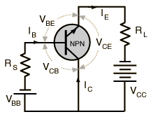
Common collector amplifier (earlier version is referred to in discussion)
Collector resitors are not normally used in CC ccts are they.
THis diag needs altering by someone who can do it.Light current 22:59, 6 August 2005 (UTC)Reply
It's a diagram of the most general case. Set Rc to 0 if you don't want it there. - Omegatron 14:21, August 7, 2005 (UTC)
We could put in all sorts of extra components that are not needed and set their impedance to either 0 or infinity as required but I feel that, whilst you and I may be able to understand it, it would confuse the issue for the general reader.
Everything should be as simple as possible ( but no simpler) A. Einstein Light current 23:04, 7 August 2005 (UTC)Reply
Please refer to Horowitz and Hill's The Art of Electronics Ch.2 (transistors)for a good run down on emitter followers. Generally, they do NOT show resistors in the collector and I think we should follow them. Light current 01:19, 8 August 2005 (UTC)Reply
On this occasion, I tend to agree, most emitter follower circuits simply connect the collector to the supply rail, and though in the general case they might have a resistor, in practice they almost never do. I think simpler diagrams are better. The same wpould apply to the common base diagram - it is more obvious to lay it out with the base clamped to 0v and the transistor turned so that the input is on the left, the output on the right. Graham 01:40, 8 August 2005 (UTC)Reply
Yes. The reason I used this layout was to show the similarities between the three configurations. It's not obvious to a newcomer who sees the sideways version that they are all variations on a theme:
I can draw a sideways common base, too, if everyone wants, and we can put them both in the common base article? And I'll delete the resistor and cap from this image if you insist, although if it is ever used in practice, it should really stay. - Omegatron 02:12, August 8, 2005 (UTC)
The diagrams are very nice actually, but I feel that deliberately making them all look the same might tend to obfuscate rather than enlighten, since to the casual observer the key differences are not obvious. Remember that electronics engineers will already know this stuff, so it needs to be aimed at a lay-audience. Personally I'd leave out the bias network, and just illustrate the circuits with the bare minimum of components, which basically means that only the load resistor should be shown. Waveforms to show phase and gain relationships, and perhaps arrows pointing "into" the inputs and outputs giving the impedance (high/low is all that's needed) would also help. This is all I did in my diagrams over at electronic amplifier, though I notice that I've recently come in for some criticism there. My belief is that simpler is best (but no simpler than necessary of course) and while these circuits can be made to look the same, it is probably more helpful if their differences are exaggerated. Graham 02:35, 8 August 2005 (UTC)Reply
Must say I totally agree with everything Graham is saying. Light current 05:26, 8 August 2005 (UTC)Reply
Yes I would like O'tron to do sideways version of CB as this tends to be the way its normally drawn (unless part of a cascode). Can you draw one of those as well while you're at it?? Light current 05:38, 8 August 2005 (UTC)Reply
I disagree with stripping important components off it unless we're showing a small-signal model. - Omegatron 10:57, August 8, 2005 (UTC)
There's nothing wrong with showing several circuits on the page. They're real easy to make. We can show an actual practical circuit, a small-signal model, show various transistormodels on the BJT page, etc.
I'm going to redo all the schematics with proper subscripts later today. (I was in a rush when I made these articles.) Is there anything else I should change in these ones while I'm doing it? (The sideways CB will be a different file.) - Omegatron 12:51, August 8, 2005 (UTC)
Compromise suggestion. would it be possible to draw the bias components in 'greyed out' form so that they are visible but not prominent. THese components could then be referred to if necc in the text. Light current 13:57, 8 August 2005 (UTC)Reply
I think that's an excellent idea - I guess we are so used to the limitations of printed paper that the idea of taking advantage of our medium (web pages) to do something different rarely occurs. However I'd also be happy with multiple diagrams - perhaps one which just shows the very bare essentials, and another that is a practical circuit. Graham 22:58, 8 August 2005 (UTC)Reply
Hmm.. Let's think about what we want exactly before I redraw anything. They're relatively easy to draw, but I don't want to waste my time doing something and then changing it later.
In defense of my images, here's the book I learned from (though it's been a while):
Microelectronic Circuits by Adel S Sedra, K C Smith, Third edition. The word "universal" only appears twice in the most recent, fifth edition, and not next to the word amplifier, so they've apparently abandoned this particular teaching method... :-)
How about I make a version of the universal amplifier and we can mention it, and then change the three current images to represent the most typical cases? Then we can add some other things like small-signal models or your stripped down unbiased versions. Then everyone will be happy. Give me a roadmap of what images you want, though. - Omegatron 23:54, August 8, 2005 (UTC)
Oh! Yes greyed-out components would be great and save some room. Just the bias resistors or the caps too? - Omegatron 23:56, August 8, 2005 (UTC)
Isay just the bias chain. THe capacitors are part of the signal path. But I'm not fussy (who said?) it depends on the accomp text really. :-)Light current 00:07, 9 August 2005 (UTC)Reply
Well we can always change the grayed part. Find some images [1][2][3] you'd like to emulate or describe the circuits you'd like to show, with exactly the components you want, and we can decide which ones to gray out later. - Omegatron 00:42, August 9, 2005 (UTC)
I like this one for emitter follower. hyperphysics.phy-astr.gsu.edu/.../ npncc.html
Sorry I do not know how to make this into a link. Will let u know of the others as I find them Light current 00:53, 9 August 2005 (UTC)Reply
THe one youve already got is OK for CE, IMHO Light current 01:01, 9 August 2005 (UTC)Reply
Added the CC image. Naming convention is the same as the original but removed the collector resistor/capacitor. The image is the one most commonly used to depict CC stages. I hope it is OK for inclusion in the article. Rohitbd 13:02, September 12, 2005 (UTC)
Latest comment: 16 years ago1 comment1 person in discussion
The previous circuit and the corresponding expressions were too complicated to be useful (IMHO). They're much simpler now without all the biasing details. I do think its important to show a practical circuit though, so I'd like to add another section maybe showing the previous circuit and explaining the biasing (the simple formulas will still be valid once you account for loading). Roger 03:55, 30 May 2007 (UTC)Reply
Latest comment: 4 years ago7 comments4 people in discussion
I think the small-signal characteristics should be grouped together in a table. I don't have any experience with wiki-tables, but I just came up with this:
I just put the approximate expression in a different column. I could also put the definition of each function in a separate column (e.g. a column with only Av = Vo/Vi next to "Voltage gain"). Comments? Roger 03:54, 30 May 2007 (UTC)Reply
That looks better, thanks. If no one else has any ideas I'll start incorporating that one. Roger 16:41, 18 June 2007 (UTC)Reply
Very good concept. — Omegatron 20:11, 5 August 2007 (UTC)Reply
I think we should include the simpler approximations in the text itself, though, and segregate the more specific models to their own section, as I've tried to do to this one. (Or maybe give each transistor model its own article?) — Omegatron 22:35, 5 August 2007 (UTC)Reply
I think using RE in the gain formula is misleading. RE is the emitter resistor, while in the formula we need RE parallel with Rload. Also, the approximation for Av=1 is true for the criteria mentioned in the table. However, the whole idea of the CC circuit is to drive very low impedance loads, because it has a low output impedance, allowing for high output power. Now if you try this circuit with matched load (Rload=rout) then you'll notice the Av becomes 0.5 (ideally, in reality it will be somewhat different, but still much less than one). This is not mentioned in many pages and books discussing this circuit, I don't know why... (of course in reality the push-pull variation is used for power amps, but has the same concept) Hoemaco (talk) 12:17, 24 April 2020 (UTC)Reply
Latest comment: 16 years ago2 comments2 people in discussion
Rout is deficient by the absence of re (the internal resistance of the emitter). This is equal to 25/Ie ohms where Ie is in mA. This should be added to the expression for Rout for correctness. —Preceding unsigned comment added by 88.109.121.209 (talk) 00:27, 7 October 2007 (UTC)Reply
"re" is equal to 1/gm (where gm is IC/VT), so the current expression is indeed correct (look in the " Approximate expression" column). -Roger 06:35, 7 October 2007 (UTC)Reply
Latest comment: 13 years ago13 comments4 people in discussion
A voltage follower is not a negative feedback circuit. I reverted C-F's edits concerning this Original Research WP:OR of his. What C-F thinks is negative feedback is actually due to the Miller Effect, a product of the Beta or current gain of a transistor. Zen-in (talk) 17:02, 10 May 2010 (UTC)Reply
Zen-in, I wonder why you do not understand so simple circuit concepts! How this is possible? The emitter follower and the op-amp follower are the most elementary circuits with series negative feedback. The Miller integrator and the op-amp inverting integrator are circuits with parallel negative feedback. The two negative feedback configurations have different properties regarding the input resistance, inverting/non-inverting abilities, etc. Let's discuss this topic! Circuit dreamer (talk, contribs, email) 17:41, 10 May 2010 (UTC)Reply
Before doing all these edits you should have discussed them here. Instead you decided to unilaterally modify several pages with content that is possibly WP:OR and is your own POV. The Miller effect, also referred to as Miller feedback is a different concept. Calling the Miller effect negative feedback confuses the concept. In the Miller effect article negative feedback amplifiers are discussed. There is a very clear distinction between the Miller effect and negative feedback. The first is a function of the inherent current gain of transistors and the other is usually a multi-stage circuit. Not long ago you were trying to show that negative resistance was the root cause for a lot of "mysterious" electronic phenomena. Now it seems you have gotten on the negative feedback bandwagon. Zen-in (talk) 19:56, 10 May 2010 (UTC)Reply
Zen-in, you know very well that I have written a big mass of text on the discussion pages (if you have forgotten, see my contributions). But it resulted in nothing just because you and people like you do not want to think and only convey blindly banal knowledge to Wikipedia. The result is more than deplorable and this section is a good example of this paradox - to know so much but to understand so little. Even the simplest and the most elementary circuit explanations as this one based only on human common sense seem as an original research to you. What does it mean to say "a voltage follower is not a negative feedback circuit" when the voltage (emitter, source, cathode, op-amp, etc.) follower is exactly the most elementary negative feedback circuit? And what does it mean to say "calling the Miller effect negative feedback confuses the concept" if it implies exactly a negative feedback (an element connected between the output and the input of an inverting amplifier)?
You regularly make fun of negative resistance (impedance) phenomenon and you haven't made any efforts to understand the simple truth about it. But there is negative impedance even in the Miller integrator mentioned above by you because the output voltage of the inverting amplifier is a "mirror" copy of the voltage drop across the capacitor. The inverting amplifier acts as a "negative capacitor" that produces voltage VC instead to consume a voltage drop VC. This voltage compensates the voltage drop across the capacitor and, as a result, a virtual ground appears at the amplifier's input. Will you understand this simple truth based only on KVL (VC - VC = 0)? Well, I can understand that you can't understand circuits because they are not your vocation. But I can't understand why you do not want people to learn about simple circuit concepts, why you impede me to say the simple truth about circuits to people... Circuit dreamer (talk, contribs, email) 22:01, 10 May 2010 (UTC)Reply
Of course! Everyone but you is so totally mixed up and stupid we all can't understand these basic truths that you are elucidating - NOT! I read over your "Basic Idea" section and it is entirely your own WP:OR. Transistors commonly have a Beta of 10 - 250, never 1. I think you are the one who does not get it. As to vocations, I have studied electronics for almost 55 years and I earned a degree at a very reputable Engineering university almost 30 years ago. I have also worked in the industry for over 35 years. You should stop insulting other editors. A while ago you complained about a perceived insult from me. You have persisted to write much worse things about me, since then. If Wikipedia is becoming too upsetting maybe you need a wiki-break. Your recent edits should be reverted, but I will wait for other editors to weigh in on this. Zen-in (talk) 23:07, 10 May 2010 (UTC)Reply
In these explanations, β represents the attenuation of the negative feedback (see Fig. 2). Actually, the figure should not contain β box (there is no attenuation in this 100% negative feedback system). Circuit dreamer (talk, contribs, email) 23:20, 10 May 2010 (UTC)Reply
You said β represents something else; then you say it shouldn't be there. So you are confused about something you wrote. I rest my case. Zen-in (talk) 01:15, 11 May 2010 (UTC)Reply
Yes, the confusion is the fact that β is being used to refer to two different concepts (both of which are gains!). I would recommend eliminating β from the section on -ve feedback (including editing the image to remove the feedback box), because as you say, it's unity-gain in this case. Oli Filth(talk|contribs) 07:22, 11 May 2010 (UTC)Reply
Actually CF is correct, there is negative feedback in the CC. I'm not sure it's worth emphasizing that fact too much, since I personally don't think it's necessary for understanding this circuit. -Roger (talk) 01:56, 11 May 2010 (UTC)Reply
Sure, it's called Miller feedback but that is completely different from a feedback amplifier, which is a purposely designed circuit. Negative feedback, in the context of circuit analysis refers to a purposefully designed circuit, not a characteristic of the active elements. Zen-in (talk) 02:50, 11 May 2010 (UTC)Reply
I've never heard that topology referred to as Miller feedback, but regardless, the circuit does provide the benefits of negative feedback (higher Zin, stable gain, etc.) I see no problem with labeling it as such (several textbooks do IIRC), but (again) I don't think it necessarily needs to be emphasized. -Roger (talk) 03:21, 11 May 2010 (UTC)Reply
I think it is only recently the term Miller Feedback has come into use. But it is a mistake to reassign the Miller Effect as a fundamental basic manifestation of negative feedback as C-F wants to do. The problem comes when you are discussing feedback amplifiers. What feedback are you talking about? Also in C-F's edits to this page he is introducing a lot of WP:OR, like alternative uses for β that even C-F is uncertain of, and comparisons to op-amp configurations. This POV is being spread thickly over several unrelated pages. Granted it isn't as bad as the stick men diagrams we used to see, but WP:OR it is. So instead of questioning my one edit why aren't you talking to C-F about all of his? Am I to assume you will always be his apologist? Zen-in (talk) 06:13, 11 May 2010 (UTC)Reply
I wasn't trying to be his apologist, I just wanted to address your comment that there wasn't NFB in the CC circuit (there is, due to the emitter resistance; just as in the CE). As I've said, I don't think this needs to emphasized in the article at all, so I didn't want to bring up a whole OR discussion again. -Roger (talk) 16:19, 11 May 2010 (UTC)Reply
Latest comment: 13 years ago23 comments4 people in discussion
The statement " The output current (and thus the output voltage) is determined by the voltage across the transistor's base-emitter junction " is incorrect. A BJT is current-driven. The collector current is a function of the base current, ie: IC = β*IB. VBE is a function of process, temperature and base current. This effort of trying to explain a transistors behavior with negative feedback is causing incorrect information to be added to this page. While intuitively you can look at it that way one problem is that there is just the one active device which somehow is both an amplifier and a de-amplifier (negative feedback). This, by itself, points out the ludicrous nature of this position. Zen-in (talk) 01:31, 12 May 2010 (UTC)Reply
I believe the voltage controlled and current controlled models are both alternate but equally valid viewpoints, see also the BJT article. I agree about the NFB stuff though. It might be one way of understanding this simple circuit, but I don't think it's particularly helpful. A cited sentence or two might be acceptable though. -Roger (talk) 01:45, 12 May 2010 (UTC)Reply
Feel free to do as you wish with my version of the -ve feedback stuff; I reduced it to two sentences as a compromise in order to reduce its prominence. However, Zen-in; please accept that you're wrong sometimes! The -ve feedback view is perfectly valid, so please stop hammering on as if it weren't. However, I agree with Roger, the usefulness of the -ve feedback model may be questionable.
And I'm not sure what you're going with "just one active device". There's only one active device in an op-amp -ve feedback amplifier; the "de-amplification" is achieved with the external network. Oli Filth(talk|contribs) 07:11, 12 May 2010 (UTC)Reply
A transistor is "just one active device", and an op-amp has many. My point is that negative feedback involves a gain-producing element and gain-reducing feedback. In a CC circuit the two are the same. The only place where negative feedback has any relevance to single transistor stages is the CE circuit where there is an emitter resistor that isn't bypassed. But that has always been called emitter degeneration. Zen-in (talk) 16:11, 12 May 2010 (UTC)Reply
An op-amp is a single active device in that it has a single (differential) input and a single output. And no, in the CC circuit, the gain-producing element is the transistor's transconductance; the feedback network is the emitter resistor. And this is the same mechanism as emitter degeneration, which is referred to (correctly) as negative feedback in the Common emitter article! Oli Filth(talk|contribs) 16:20, 12 May 2010 (UTC)Reply
I have not seen any BJT models that are voltage controlled and I haven't seen any case where this is considered in a device physics textbook. The Wikipedia BJT article doesn't cite any references except Horowitz and Hill, where they mention that BJTs are current amplifiers and FETs are voltage controlled. Zen-in (talk) 16:11, 12 May 2010 (UTC)Reply
gm is the small-signal parameter that relates input voltage to output current for a BJT. Please see Transconductance. Oli Filth(talk|contribs) 16:20, 12 May 2010 (UTC)Reply
The AoE is not really the authoritative reference on transistors, but it does say "... it is important to realize that the collector current is accurately determined by the base-emitter voltage, rather than by the base current ..." -Roger (talk) 16:28, 12 May 2010 (UTC)Reply
I suppose you can look at BJTs either way since both are non-linear responses. However gm varies exponentially with VBE while β does not change very much over the range of the base current of BJTs. That is why β is more commonly used when designing circuits with BJTs and gm used with FETs. The AoE statement you quote is correct but most of us prefer to use a less accurate β that is almost a constant value than the exponential gm. Zen-in (talk) 18:24, 12 May 2010 (UTC)Reply
Zen-in: "However gm varies exponentially with VBE while β does not change very much over the range of the base current of BJTs."
Right, but g_m (I_C/V_T) is much more predictable than \beta, and most designs fix I_C and are have an expected range for V_T. \beta also varies quite widely with temperature and current. -Roger (talk) 19:31, 12 May 2010 (UTC)Reply
Oli Filth (this is a reply to your previous insertion above), you have gone too far; please, stop playing the demagogue! First, you reminds Zen-in that "he is wrong sometimes" although you know perfectly that, as a rule, he is wrong every time when he tries to do something different than removing! Then you ask him "to stop hammering on the -ve feedback view as it is perfectly valid" but, at the same time, you have removed almost everything written about it and inserted only these two vague and scanty sentences somewhere between the text and expressions!
But this is the most elementary system with negative feedback, the base of the negative feedback theory; so, we have to show precisely how it puts in practice the powerful negative feedback idea. Although it (frequently) contains only one transistor, it is not so easy to see a negative feedback here. As we can see, even people that "have studied electronics for almost 55 years and earned a degree at a very reputable Engineering university...and also worked in the industry for over 35 years" do not see any negative feedback here! How do we expect then technicians, pupils, students and just curious young people to understand it?
Well, once we accept the negative feedback approach, we have first to show the functional block-diagram of the most elementary negative feedback system with its inherent components: a power supply (not obligatory but preferable), a regulating element (a non-inverting amplifier in this case) and a subtractor. In this figure, we have to designate also the according quantities: the input voltage VIN, the amplifier's output voltage VOUT and the subtractor's output voltage (the amplifier's input voltage) Vdiff = VIN - VOUT.
Then, we have to show, clearly and precisely, how each of these components is implemented in the specific BJT voltage follower (to make the connection between the general components and the specific circuit elements): the power supply V+ (more precisely, VCC), the transistor and the series subtracting loop.
Finally, we have to describe thoroughly the operation of this elementary negative feedback follower. The paradox is that if we think of the active device (a transistor here) as of a non-inertial, proportional, instantaneous device (i.e., as of a transistor:), we will fall into a vicious circle and we will never understand the negative feedback mechanism (most likely, we will decide that this circuit is an inverting amplifier (see the discussion about Schmidt triggers:) The only way to understand a feedback circuit is to think of the active device as of a slow (integrating) device what it actually is at very high frequencies. Like a "human being" (empathy), it "observes" the result of comparison between the input and output voltage and changes the output voltage (by passing a current through the emitter resistor) so that to zero the voltage difference. Here we have to show the use of applying negative feedback, to emphasize the unique negative feedback feature to suppress of all kinds disturbances that tend to change the output voltage.
I have reorganized the article according to these considerations. I have restructured the first part since the most text of the voltage buffer section should belong to the basic emitter follower section (it is not appropriately to start the article directly by circuit applications). Circuit dreamer (talk, contribs, email) 16:45, 12 May 2010 (UTC)Reply
I reduced the -ve feedback stuff because it was totally excessive. It is not the most effective way of viewing how the CC circuit works (the small-signal analysis is simpler and more generic). As Roger has said, it's barely worth mentioning in the article at all; my two sentences were a compromise that contained all the essential information. Currently, that's 2 vs 1, so I'm going to revert your change soon unless you can come up with a convincing reason why we need to go to these lengths (hint: what you've just written above is not at all convincing!). Oli Filth(talk|contribs) 16:50, 12 May 2010 (UTC)Reply
C-F: can you consider putting that NFB stuff in the negative feedback amplifier article, where it's probably better suited? This article should really be about explaining the CC stage as concisely as possible, without requiring a background in feedback. A couple sentences and a link to the NFB article is sufficient IMHO. -Roger (talk) 17:05, 12 May 2010 (UTC)Reply
Of course but, as you can see, this is not the problem. The big problem is first to persuade reliable wikipedians (including you) in benefits of applying this approach. Thanks for the moral support; it happens seldom. Circuit dreamer (talk, contribs, email) 17:11, 12 May 2010 (UTC)Reply
(outdent) Incidentally, I agree with your article restructuring, but not with the verbosity of the -ve feedback stuff. Oli Filth(talk|contribs) 17:43, 12 May 2010 (UTC)Reply
You are native english speaker; so, you can say it better. I have nothing against rewording and shortening the text if only you manage to keep the main points. But let's first assess the situation very well, to decide what is more important - to explain the circuit thoroughly or to show how to calculate it precisely. Circuit dreamer (talk, contribs, email) 18:03, 12 May 2010 (UTC)Reply
" to explain the circuit thoroughly or to show how to calculate it precisely " Both are equally important and have already been accomplished in this article by using time-proven and generally accepted circuit analysis methods. Zen-in (talk) 18:29, 12 May 2010 (UTC)Reply
I agree with Zen-in on this. I have yet to come across a textbook that introduces basic transistor amplifier stages along with feedback. Emphasizing the NFB approach on an introductory topic like this probably doesn't help the uninitiated too much. Plus the loop gain is so low that it's hard to identify the unilateral feedback model parameters, so this approach won't help you solve practical problems. -Roger (talk) 20:06, 12 May 2010 (UTC)Reply
Negative feedback is the most familiar phenomenon for the uninitiated as we, human beings, act exactly as "negative feedback followers" in our routine: first, we set some aim (input quantity); then we begin realizing it by doing something (output quantity) and continuously comparing the two quantities; finally, we stop when they become equal. The same general approach can be used for explaining op-amp, FET, tube, etc. circuits. Maybe, you are right that this approach won't help readers solve practical problems; but it will help them understanding these circuits. Circuit dreamer (talk, contribs, email) 22:49, 12 May 2010 (UTC)Reply
I would like to add some comments to the discussion above. I am not sure how to indent this insertion; so, I will outdent. Circuit dreamer (talk, contribs, email) 22:24, 12 May 2010 (UTC)Reply
How do we drive the transistor? We may control a bipolar transistor both by voltage and current. If we drive it by voltage (a CE stage is a good example), we obtain maximum gain (+) and nonlinearity (-) and minimum input range (-) and resistance (-). To drive the transistor by current (a transistor switch is a good example), we have to connect a base resistor acting as a voltage-to-current converter. As a result, the gain (-) and the nonlinearity decrease (+), the input range (+) and the input resistance increase (+). In the emitter follower, the transistor is voltage-driven but this configuration does not have the disadvantages above since: the nonlinearity is not significant because it is compensated by the negative feedback; the low input resistance (because of the bootstrapping) and the input range (because of the "self-movable" ground) are increased artificially by the series negative feedback.
What are gain-producing and de-amplifier elements? The voltage-driven transistor (transconductance amplifier) and the emitter resistor (current-to-voltage converter) constitute a voltage amplifier with a differential input where the base is the inverting input and the emitter is both the non-inverting input and the output. The non-inverting input and the output are connected "naturally"; so, the feedback "network" is just a piece of wire - the common point between the bottom terminals of the base-emitter and collector-emitter junctions.
What is the connection between the emitter follower and a CE amplifier with emitter degeneration? If we use the emitter as an output, this is an emitter follower. In this configuration, the collector resistor is suppressed by the negative feedback and does not influence the emitter follower (it can act as a current-protecting resistor that is "hidden" by the negative feedback; see TTL totem-pole output stage). But, at some input voltage, the transistor will saturate since, figuratively speaking, the emitter and the collector voltages "move" against to each other and, at some moment, they "meet". If we use the collector as an output, this is the very inverting amplifier with emitter degeneration. We may use the both outputs as a non-inverting and an inverting output (see TTL second stage). Circuit dreamer (talk, contribs, email) 22:24, 12 May 2010 (UTC)Reply
CF: sorry, I'm not sure what point you're trying to make with your comment, or who it's addressed to. Also try to be a bit more concise. EDIT: Sorry again, it seems you were addressing my previous comment. Perhaps I should have said "quantitatively identify the unilateral feedback model parameters", a point which still stands (see asymptotic gain model) -Roger (talk) 22:49, 12 May 2010 (UTC)Reply
I have just collected here a few opinions (comments) about the topics that are discussed above in this section. I hope I have added useful thoughts. Circuit dreamer (talk, contribs, email) 23:02, 12 May 2010 (UTC)Reply
Latest comment: 13 years ago3 comments2 people in discussion
Does anyone else think the derivation section might be a bit too detailed? I'm thinking about pruning it down. -Roger (talk) 20:49, 13 May 2010 (UTC)Reply
Some people don't want to see any math; I'm the opposite. If there are any duplications or errors they should be fixed or deleted; but that doesn't seem to be the case. IMHO the derivation section is a good example of what most electronics article should include. No need to prune from something that is well done and correct. Zen-in (talk) 00:12, 14 May 2010 (UTC)Reply
I get what you're saying, but at the same time the derivations are fairly straight forward and easy to find in a textbook (which Wikipedia is not). Perhaps we could include them in a collapsible side panel (I remember seeing something like that in some other article) instead? -Roger (talk) 01:02, 14 May 2010 (UTC)Reply
Latest comment: 8 years ago1 comment1 person in discussion
The article explains that "In this circuit the base terminal of the transistor serves as the input, the emitter is the output, and the collector is common to both (for example, it may be tied to ground reference or a power supply rail), hence its name".
This doesn't make sense to me. Can somebody explain what is meant by common?
Latest comment: 6 years ago1 comment1 person in discussion
Hello fellow Wikipedians,
I have just modified 2 external links on Common collector. Please take a moment to review my edit. If you have any questions, or need the bot to ignore the links, or the page altogether, please visit this simple FaQ for additional information. I made the following changes:
When you have finished reviewing my changes, you may follow the instructions on the template below to fix any issues with the URLs.
This message was posted before February 2018. After February 2018, "External links modified" talk page sections are no longer generated or monitored by InternetArchiveBot. No special action is required regarding these talk page notices, other than regular verification using the archive tool instructions below. Editors have permission to delete these "External links modified" talk page sections if they want to de-clutter talk pages, but see the RfC before doing mass systematic removals. This message is updated dynamically through the template {{source check}} (last update: 18 January 2022).
If you have discovered URLs which were erroneously considered dead by the bot, you can report them with this tool.
If you found an error with any archives or the URLs themselves, you can fix them with this tool.


