This article needs additional citations for verification. (December 2011) |
A quad flat package (QFP) is a surface-mounted integrated circuit package with "gull wing" leads extending from each of the four sides.[1] Socketing such packages is rare and through-hole mounting is not possible. Versions ranging from 32 to 304 pins with a pitch ranging from 0.4 to 1.0 mm are common. Other special variants include low-profile QFP (LQFP) and thin QFP (TQFP).[2]

The QFP component package type became common in Europe and United States during the early nineties, even though it has been used in Japanese consumer electronics since the seventies. It is often mixed with hole mounted, and sometimes socketed, components on the same printed circuit board (PCB).
A package related to QFP is plastic leaded chip carrier (PLCC) which is similar but has pins with larger pitch, 1.27 mm (or 1/20 inch), curved up underneath a thicker body to simplify socketing (soldering is also possible). It is commonly used for NOR flash memories and other programmable components.
Limitations edit
The quad flat-pack has connections only around the periphery of the package. To increase the number of pins, the spacing was decreased from 50 mil (as found on small outline packages) to 20 and later 12 (1.27 mm, 0.51 mm and 0.30 mm respectively). However, this close lead spacing made solder bridges more likely and put higher demands on the soldering process and alignment of parts during assembly.[1] The later pin grid array (PGA) and ball grid array (BGA) packages, by allowing connections to be made over the area of the package and not just around the edges, allowed for higher pin counts with similar package sizes, and reduced the problems with close lead spacing.
Variants edit
-
 144-pin low profile quad flat package (LQFP)
 -
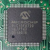 80-pin thin quad flat package (TQFP) – PIC microcontroller
 -
 304-pin plastic quad flat package (QFP) with exposed thermal pad (TP)
 -
 100-pin bumpered quad flat package (BQFP) – Cyrix Cx486SLC
 -
 80-pin ceramic quad flat package (TQFP) – ST6 microcontroller
.jpg)


The basic form is a flat rectangular (often square) body with leads on four sides but with numerous variation in the design. These differ usually only in lead number, pitch, dimensions, and materials used (usually to improve thermal characteristics). A clear variation is bumpered quad flat package (BQFP) with extensions at the four corners to protect the leads against mechanical damage before the unit is soldered.
Heat sink quad flat package, heatsink very thin quad flat-pack no-leads (HVQFN) is a package with no component leads extending from the IC. Pads are spaced along the sides of the IC with an exposed die that can be used as ground. Spacing between pins can vary.
A thin quad flat pack (TQFP) provides the same benefits as the metric QFP, but is thinner. Regular QFP are 2.0 to 3.8 mm thick depending on size. TQFP packages range from 32 pins with a 0.8 mm lead pitch, in a package 5 mm by 5 mm by 1 mm thick, to 256 pins, 28 mm square, 1.4 mm thick and a lead pitch of 0.4 mm.[2]
TQFPs help solve issues such as increasing board density, die shrink programs, thin end-product profile and portability. Lead counts range from 32 to 176. Body sizes range from 5 mm x 5 mm to 20 x 20 mm. Copper lead-frames are used in TQFPs. Lead pitches available for TQFPs are 0.4 mm, 0.5 mm, 0.65 mm, 0.8 mm, and 1.0 mm. PQFP, or plastic quad flat pack, is a type of QFP, as is the thinner TQFP package. PQFP packages can vary in thickness from 2.0 mm to 3.8 mm. A low-profile quad flat package (LQFP) is a surface mount integrated circuit package format with component leads extending from each of the four sides. Pins are numbered counter-clockwise from the index dot. Spacing between pins can vary; common spacings are 0.4, 0.5, 0.65 and 0.80 mm intervals.
| Package | description |
|---|---|
| BQFP | bumpered quad flat package |
| BQFPH | bumpered quad flat package with heat spreader |
| CQFP | ceramic quad flat package |
| EQFP | plastic enhanced quad flat package |
| FQFP | fine pitch quad flat package |
| LQFP | low profile quad flat package |
| MQFP | metric quad flat package |
| NQFP | near chip-scale quad flat package.[3] |
| SQFP | small quad flat package |
| TQFP | thin quad flat package |
| VQFP | very small quad flat package |
| VTQFP | very thin quad flat package |
| TDFN | thin dual flat no-lead package.[4] |
Some QFP packages have an exposed pad. The exposed pad is an extra pad underneath or on top of the QFP that may act as a ground connection and/or as a heat sink for the package. The pad is typically 10 or more mm2, and with the pad soldered down onto the ground plane, heat is passed into the PCB. This exposed pad also gives a solid ground connection. These type of QFP packages often have a -EP suffix (e.g. a LQFP-EP 64), or they have an odd number of leads, (e.g. a TQFP-101).
Ceramic QFP package edit
Ceramic QFP packages come in two variants, CERQUAD and CQFP:
CERQUAD packages edit
Hereby the leadframe is attached between two ceramic layers of the package. The leadframe is attached using glass. This package is a variant of the CERDIP package. CERQUAD packages are the "low cost" alternative for CQFP packages, and are mainly used for terrestrial applications. Main ceramic package manufacturers are Kyocera, NTK,... and offer the full pincount range
CQFP packages edit
Hereby the leads are soldered on top of the package. The package is a multilayer package, and is offered as HTCC (high temperature co-fired ceramic). The number of bonding decks can be one, two or three. Package is finished with a nickel plus a thick gold layer, except where the leads are soldered and decoupling capacitors are soldered on top of the package. These packages are hermetic. Two methods are used in order to make the hermetic sealing: eutectic gold-tin alloy (melting point 280 °C) or seam welding. Seam welding gives rise to significantly less temperature rise in the internal of the package (e.g., the die attach). This package is the main package used for Space projects.
Due to the large body size of CQFP packages, parasitics are important for this package. Power supply decoupling is improved by having the decoupling capacitors mounted on top of this package. E.g. TI offers 256-pin CQFP packages where decoupling capacitors can be soldered on top of the package[5] E.g. Test-expert 256-pin CQFP packages where decoupling capacitors can be soldered on top of the package.[6]
The main ceramic package manufacturers are Kyocera (Japan), NTK (Japan), Test-Expert (Russia), etc. and offer the full pincount range. Maximum pin count is 352 pins.
See also edit
- Chip carrier
- Pin grid array - an alternative integrated circuit pin arrangement design
- Dual in-line package
References edit
- ^ a b Greig, William J. (2007). Integrated circuit packaging, assembly and interconnections. Springer. pp. 35-26. ISBN 978-0-387-28153-7.
- ^ a b Cohn, Charles; Harper, Charles A., eds. (2005). Failure-free integrated circuit packages. McGraw-Hill. pp. 22–28. ISBN 0-07-143484-4.
- ^ "AMIS-492x0 Fieldbus MAU Datasheet" (PDF).
- ^ "AAT3620 Datasheet" (PDF).
- ^ "Ceramic Quad Flatpack (CQFP)" (PDF).
- ^ "Корпус микросхемы МК 4244.256-3 (тип CQFP)".